





High Temperature Co-Fired AlN (HTCC): Thermal Conductivity, Multi-Layer DFM, and Machining Guide
Custom High temperature co-fired AlN (HTCC) substrates provide 170–200 W/(m·K) thermal conductivity, tungsten circuit integration, matched silicon CTE, and sub-micron lapping for RF/semiconductor modules.
High Temperature Co-Fired AlN (HTCC): Thermal Conductivity, Multi-Layer DFM, and Machining Guide
When high-power silicon carbide (SiC) and gallium nitride (GaN) power modules burn out from chronic thermal choking, conventional alumina packaging cracks catastrophically. Consequently, hardware architects specify High temperature co-fired AlN (HTCC) to dissipate extreme heat fluxes while providing embedded high-voltage isolation.
What is High temperature co-fired AlN (HTCC)? High temperature co-fired AlN (HTCC) is an advanced multi-layer ceramic packaging technology that co-fires high-purity aluminum nitride (AlN) tape-cast green sheets together with refractory tungsten (W) or molybdenum (Mo) conductive metallization traces at temperatures between 1800°C and 1900°C in a reducing atmosphere. Delivering an exceptional bulk thermal conductivity of 170–200 W/(m·K), matched silicon thermal expansion (4.5 × 10^-6 /K), dielectric strength above 15 kV/mm, and hermetic metallized vias, High temperature co-fired AlN (HTCC) serves as the definitive substrate platform for high-reliability optoelectronics, aerospace radar, and semiconductor wafer-handling heaters.
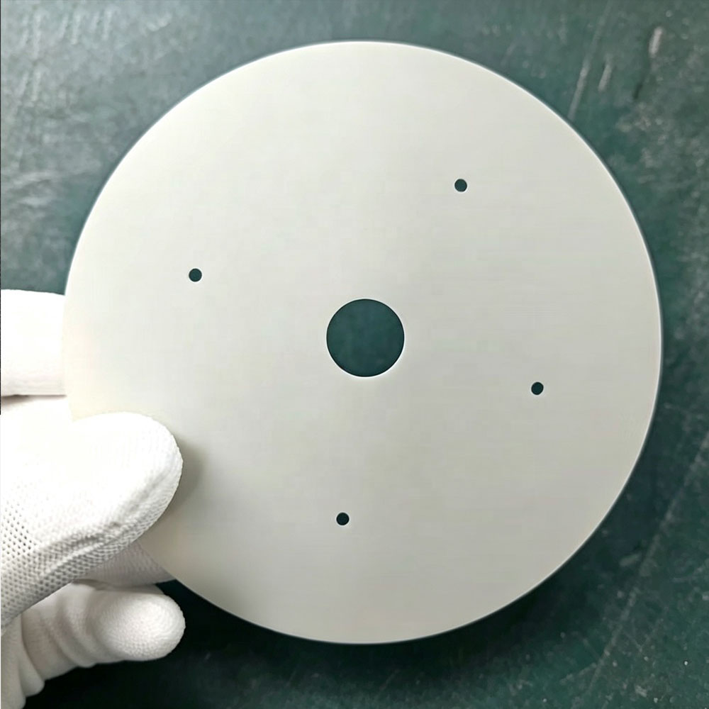
The Physics & Chemistry Behind the Performance: Lattice Phonons and Co-Firing Sintering
Unlike metals that conduct thermal energy via free electron clouds, aluminum nitride transfers thermal kinetic energy strictly through crystal lattice vibrations, which physicists call acoustic phonons. Therefore, optimizing pure AlN lattice chemistry determines heat transfer performance directly.
Aluminum nitride crystallizes in a hexagonal wurtzite lattice characterized by strong covalent bonds with high bond energy. However, trace oxygen impurities displace nitrogen in the wurtzite lattice, creating aluminum vacancies that aggressively scatter acoustic phonons. Consequently, oxygen contamination drops raw AlN thermal conductivity from its theoretical 320 W/(m·K) down to less than 100 W/(m·K).
To eliminate this scattering mechanism, process engineers introduce precise concentrations of yttrium oxide (Y2O3, ~3–5 wt%) as a liquid-phase trapping agent during sintering. Specifically, the Y2O3 liquid phase reacts with surface alumina layers at 1850°C, forming stable yttrium-aluminate secondary phases (such as YAG and YAP) at triple-point grain boundaries. As a result, this reaction purges oxygen defects out of the AlN grains, enabling acoustic phonons to travel unhindered and driving thermal conductivity up to 170–200 W/(m·K).
Furthermore, because sintering takes place at extreme temperatures above 1800°C, engineers must select refractory conductors with matching thermal shrinkage. Thus, high-purity tungsten paste matches the densification kinetics of the surrounding AlN body. In contrast to low-temperature co-fired ceramics (LTCC) that rely on glass fluxes, High temperature co-fired AlN (HTCC) features a fully crystalline matrix that prevents high-temperature mechanical creep, dielectric puncture, and internal delamination.
Critical Material Properties & Real-World Engineering Benchmarks
Selecting appropriate multi-layer packaging substrates requires side-by-side parametric comparisons. Therefore, the benchmarking table below highlights High temperature co-fired AlN (HTCC) against standard Alumina HTCC (90% Al2O3), Direct Bonded Copper on AlN (DBC-AlN), and low-temperature co-fired glass-ceramics (LTCC).
| Engineering Parameter | AlN HTCC (Multi-Layer) | Alumina HTCC (90% Al2O3) | DBC AlN (Single Layer) | Standard LTCC Glass |
|---|---|---|---|---|
| Thermal Conductivity (W/(m·K)) | 170 – 200 | 18 – 22 | 170 – 180 | 2.0 – 5.0 |
| Thermal Expansion CTE (×10^-6 /K) | 4.5 – 4.7 (Matches Si/SiC) | 6.8 – 7.2 | 6.5 – 7.5 (Bimetal warpage) | 5.5 – 7.0 |
| Conductor Metallization | Tungsten (W) / Moly (Mo) | Tungsten (W) / Moly (Mo) | Direct Bond Copper (Cu) | Silver (Ag) / Gold (Au) |
| Internal Trace Sheet Resistance (mΩ/sq) | 10 – 15 (Refractory metal) | 12 – 18 | < 1.0 (Thick copper) | 2.0 – 4.0 (Noble metal) |
| Multi-Layer Routing Routing Density | High (> 15 internal layers) | High (> 20 internal layers) | Low (1-2 external layers) | Very High (> 30 layers) |
| Dielectric Breakdown Strength (kV/mm) | > 15 | > 12 | > 15 | > 10 |
| Max Operating Temp (°C, Inert) | 1,000 | 1,000 | 300 (Copper oxidizes) | 450 (Glass softens) |
| Hermeticity Seal Level (mbar·L/s) | < 1 × 10^-9 (Helium leak) | < 1 × 10^-9 | N/A (Requires frame) | < 1 × 10^-8 |
Industrial Applications & Field Operational Case Studies
1. High-Density Power Semiconductor Modules (SiC & GaN Inverters)
Modern electric vehicle traction inverters switch high voltages (> 800V) across ultra-compact wide-bandgap bare dies, generating localized thermal spikes over 300 W/cm². Standard alumina substrates throttle thermal flow, creating solder joint fatigue. Consequently, inverter designers suffer premature thermal failures during sudden acceleration cycles.
In contrast, High temperature co-fired AlN (HTCC) multi-layer packages extract heat eight times faster than alumina. Furthermore, because its coefficient of thermal expansion (4.5 × 10^-6 /K) matches silicon and silicon carbide semiconductor chips, the assembly avoids thermomechanical shear stresses. Hence, power modules survive over 100,000 extreme thermal shock cycles without interface delamination.
2. Semiconductor Wafer Processing Multi-Zone Ceramic Heaters
Atomic layer deposition (ALD) and plasma etch chambers require fast thermal ramping up to 600°C while maintaining tight cross-wafer temperature uniformity within ±0.5°C. Polymer-insulated heaters melt, while exposed metal elements sputter contamination onto processed wafers.
However, multi-layer High temperature co-fired AlN (HTCC) plates integrate buried tungsten heating coils directly within monolithic ceramic layers. Because the pure AlN exterior shields the internal tungsten traces from corrosive fluorine and chlorine cleaning gases, the heater avoids oxidation. In addition, its high lateral thermal conductivity diffuses localized hotspots, ensuring uniform thin-film deposition across 300 mm silicon wafers.
3. Hermetic RF Transceiver Housings for Aerospace Radar
Phased-array radar systems and satellite communication modules route multi-gigahertz RF power through pressurized bulkhead bulk assemblies. Therefore, engineers require packages that prevent moisture ingress while maintaining high isolation.
High temperature co-fired AlN (HTCC) housings integrate internal microstrip lines, striplines, and shielded ground planes through co-fired vertical vias. Moreover, engineers braze Kovar seal rings and feedthrough pins directly to nickel-gold plated tungsten pads, achieving hermetic leak rates tighter than 1 × 10^-9 mbar·L/s for long-term orbital missions.
Precision Machining, Sintering Tolerances & DFM (Design for Manufacturability)
Designing multi-layer components using High temperature co-fired AlN (HTCC) requires strict design rules to accommodate slurry tape shrinkage, via hole alignment, and subsequent post-sinter diamond lapping.
Multi-Layer Tape Casting & Sintering Shrinkage Management
Manufacturers produce individual layers by tape casting sub-micron AlN slurries into thin flexible green sheets (thickness: 0.1 mm to 0.3 mm). Next, precision mechanical punches or UV lasers cut micro-vias (diameter: 0.1 mm to 0.25 mm), which automated screen printers fill with conductive tungsten paste.
Subsequently, technicians stack, align, and isostatically laminate the printed layers under 15–20 MPa at 70°C. During ultimate co-firing at 1850°C in pure nitrogen, the composite stack undergoes 18% to 22% linear shrinkage. Therefore, engineers must design layer-to-layer registration using precise non-linear shrinkage models. After firing, standard as-fired dimensional tolerances adhere to ±0.8% of nominal length (minimum ±0.1 mm).
Post-Sinter Diamond Grinding, Lapping & Metallization Plating
Achieving tight mechanical tolerances on fully dense AlN HTCC substrates requires specialized post-sinter diamond finishing and electrochemical plating lines.
- Ductile-Regime Diamond Lapping: Because sintered AlN possesses moderate hardness (HV 1100–1200) and low fracture toughness (KIC ~3.5 MPa·m½), machinists use planetary diamond lapping machines to remove firing camber. This micro-abrasive process reliably delivers optical surface flatnesses within 2 helium light bands (0.6 µm) and surface finishes of Ra ≤ 0.05 µm.
- Electrolytic Plating for Solderability: Co-fired tungsten surface pads cannot accept solder alloys directly. Therefore, technicians electroplate the exposed refractory traces with 2–5 µm of electrolytic nickel followed by 0.5–1.5 µm of immersion gold (ENIG / ENEPIG), which facilitates reliable gold-tin (AuSn) die attachment and thermosonic gold wire bonding.
- Laser Scribing and CNC Dicing: Diamond saw dicing or high-precision UV laser cutting sections multi-up production panels into individual substrates, holding final perimeter tolerances down to ±0.05 mm without edge chipping.
Key DFM Design Rules for Engineers
- Maintain Balanced Conductor Symmetry: Because tungsten and AlN exhibit slight differences in thermal contraction during cooldown, asymmetric metal density between top and bottom layers induces post-sinter warpage. Therefore, designers must balance conductor volumes symmetrically throughout the substrate stack.
- Follow Standard Via Aspect Ratios: To ensure complete tungsten filling and prevent internal voids, keep the via hole diameter-to-tape-thickness aspect ratio between 1:1 and 1:2. In addition, place adjacent via centers at least two via diameters apart to avoid inter-layer cracking.
- Protect Against Moisture Hydrolysis: While fully sintered AlN resists ambient air, un-sintered powders and hot humid steam (> 100°C) slowly hydrolyze AlN surfaces into aluminum hydroxide and ammonia gas. Consequently, designers must protect exposed AlN surfaces using gold plating, glass passivation, or dry inert hermetic sealing.
Frequently Asked Questions (Engineering FAQ)
What is the difference between High temperature co-fired AlN (HTCC) and LTCC?
HTCC processes fire at 1800°C–1900°C with refractory conductors (tungsten/moly), yielding a high thermal conductivity of 170–200 W/(m·K) and high structural strength. In contrast, Low Temperature Co-Fired Ceramics (LTCC) incorporate glass fluxes that sinter at 850°C–900°C with noble metals (silver/gold), but LTCC provides very low thermal conductivity (2–5 W/(m·K)), restricting its use to low-power RF signal processing.
Can High temperature co-fired AlN (HTCC) support hermetic sealing?
Yes. Fully co-fired AlN HTCC creates a dense, non-porous hermetic structure. Because the co-fired tungsten vias and surface pads bond metallurgically to the ceramic matrix, the resulting feedthroughs routinely pass helium mass spectrometer leak tests below 1 × 10^-9 mbar·L/s, complying fully with MIL-STD-883 hermetic standards.
Why do engineers use tungsten instead of copper inside AlN HTCC?
Pure copper melts at 1084°C, which makes it chemically impossible to co-fire copper inside an AlN furnace operating at 1850°C. Therefore, manufacturers must use refractory metals like tungsten (melting point: 3422°C) or molybdenum. While tungsten exhibits higher electrical resistivity than copper, its matched sintering shrinkage and thermal expansion make it the only reliable internal conductor for high-temperature AlN co-firing.
How does AlN HTCC perform under high-voltage dielectric stress?
AlN HTCC provides excellent electrical insulation, delivering a volume resistivity exceeding 10^14 Ω·cm at 20°C and a dielectric breakdown field strength above 15 kV/mm. Furthermore, its low dielectric constant (k ~8.5–9.0 at 1 MHz) and low loss tangent (tan δ ~0.0005) prevent signal distortion and minimize dielectric heating during high-frequency switching operations.
Conclusion: Technical Trade-Offs & OEM Engineering Support
Every packaging architecture balances thermal conduction, electrical resistance, and manufacturing complexity. While Direct Bonded Copper (DBC) provides lower trace resistance for simple single-layer boards, High temperature co-fired AlN (HTCC) remains the definitive solution for applications demanding multi-layer internal routing, 180 W/(m·K) heat spreading, true hermetic reliability, and matched silicon thermal expansion.
Partnering with an experienced technical ceramics manufacturer ensures your complex multi-layer designs achieve precise layer registration without costly fabrication iterations.
Request a Technical DFM Review & Prototype Quote
Are you designing a high-power multi-layer packaging substrate, RF transceiver housing, or multi-zone ceramic heater? Submit your 2D drawings (PDF) and 3D CAD files (STEP/IGS/DXF) for an engineering DFM evaluation and quote.
- Multi-layer tape stack modeling and non-linear shrinkage compensation
- 100% electrical continuity, isolation, and CMM dimensional inspection reports
- Rapid prototyping in 15 to 20 days; certified class 10,000 cleanroom packaging lines
